

Wafer Acceptance Testing Market: Global Industry Insights and Competitive Analysis 2026-2034
The global Wafer Acceptance Testing Market, valued at a robust USD 654 million in 2025, is on a trajectory of significant expansion, projected to reach USD 1,961 million by 2032. This growth, representing a compound annual growth rate (CAGR) of 16.7%, is detailed in a comprehensive new report published by Semiconductor Insight. The study highlights the critical role of Wafer Acceptance Testing (WAT) in ensuring electrical parameter compliance, process stability, and yield optimization within advanced semiconductor manufacturing.
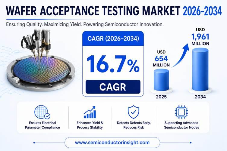
Wafer Acceptance Testing serves as a vital gatekeeping process in semiconductor production, involving precise electrical characterization of test structures on production wafers to verify that fabrication processes meet stringent design specifications before proceeding to dicing and packaging. This testing methodology enables early detection of process deviations, supports continuous yield improvement, and ensures the reliability of logic, memory, RF, and power devices across increasingly complex process nodes.
Download FREE Sample Report:
Wafer Acceptance Testing Market - View in Detailed Research Report
Semiconductor Industry Expansion: The Primary Growth Engine
The report identifies the explosive growth of the global semiconductor industry as the paramount driver for wafer acceptance testing demand. With the continued scaling of process nodes, rising complexity in chip architectures for AI, automotive, and high-performance computing applications, WAT has become indispensable for maintaining process control and product quality. The emphasis on reliability, repeatability, and traceability in electrical testing for advanced wafers further accelerates adoption.
"The massive concentration of semiconductor wafer fabs and equipment manufacturers in the Asia-Pacific region is a key factor in the market's dynamism," the report states. Global investments in new fabrication facilities continue to drive demand for sophisticated testing solutions capable of supporting sub-5nm technologies and next-generation device architectures.
Read Full Report: https://semiconductorinsight.com/report/wafer-acceptance-testing-market/
Market Segmentation: Parallel Testing and Foundry Applications Dominate
The report provides a detailed segmentation analysis, offering a clear view of the market structure and key growth segments:
Segment Analysis:
Segment Analysis:
|
Segment Category |
Sub-Segments |
Key Insights |
|
By Type |
|
Parallel Testing
|
|
By Application |
|
Foundry
|
|
By End User |
|
Logic
|
|
By Test Type |
|
Electrical Testing
|
|
By Wafer Type |
|
Logic Wafers
|
Get Full Report Here:
Wafer Acceptance Testing Market, Trends, Business Strategies 2026-2034 - View in Detailed Research Report
Competitive Landscape: Key Players and Strategic Focus
COMPETITIVE LANDSCAPE
Key Industry Players
Top Manufacturers in Wafer Acceptance Testing Equipment Market
The Wafer Acceptance Testing (WAT) market exhibits a highly concentrated structure, dominated by established leaders such as Keysight Technologies and Tektronix, which command significant market share through their advanced parametric analyzers, probe stations, and integrated software solutions. These companies benefit from strong customer stickiness among leading foundries and IDMs, driven by deep integration with process nodes, yield management frameworks, and data environments. High technical barriers, including precision measurement capabilities and lengthy qualification cycles, reinforce their positions, with gross margins typically ranging from 55% to 65%. The market's emphasis on reliability, repeatability, and traceability in electrical testing for logic, memory, RF, and power wafers further solidifies the dominance of these players in a segment projected to grow from USD 654 million in 2025 to USD 1,961 million by 2032 at a 16.7% CAGR.
Beyond the frontrunners, niche and significant players like Semitronix, Semight Instruments, and FormFactor provide specialized WAT systems, focusing on parallelism, noise suppression, and enhanced data analytics for routine production monitoring and cross-node benchmarking. Companies such as KLA Corporation and Advantest contribute probing and metrology expertise, while regional specialists including MPI Corporation and Tokyo Seimitsu (Accretech) cater to Asia-Pacific demand. Emerging challengers like Hprobe and Signatone target innovation in high-precision probing for advanced nodes, though competition remains shaped by technological depth, service capabilities, and long-term partnerships rather than frequent vendor switches. This landscape underscores the premium on software maturity and system integration amid rising automation in semiconductor fabs.
List of Key Wafer Acceptance Testing Companies Profiled
- Keysight Technologies
- Tektronix Inc.
- Semitronix Corporation
- Suzhou Semight Instruments Co., Ltd.
- FormFactor, Inc.
- KLA Corporation
- Advantest Corporation
- Teradyne, Inc.
- MPI Corporation
- Tokyo Seimitsu Co., Ltd. (Accretech)
- Hprobe
- Signatone Corporation
- MicroProbe, Inc.
These companies are focusing on technological advancements, such as enhanced automation, AI-powered data analytics, and improved probing solutions to meet the evolving requirements of next-generation semiconductor processes.
Regional Analysis: Wafer Acceptance Testing Market
Regional Analysis: Wafer Acceptance Testing Market
Asia-Pacific
The Asia-Pacific region dominates the Wafer Acceptance Testing Market, fueled by its status as the global epicenter of semiconductor manufacturing. Major hubs in Taiwan, South Korea, and China feature expansive fabrication plants from leading foundries, where rigorous wafer acceptance testing ensures high yields and defect-free production. This region's Wafer Acceptance Testing Market thrives on surging demand from consumer electronics, automotive semiconductors, and emerging AI applications. Advanced testing methodologies, including automated optical inspection and parametric electrical probing, are widely adopted to meet exacting quality benchmarks. Strategic investments by governments in domestic chip ecosystems, coupled with robust supply chains, accelerate innovation. Collaborative partnerships between equipment vendors and fab operators enhance testing precision, minimizing downtime and optimizing throughput. Despite supply chain vulnerabilities, the region's resilient infrastructure and skilled workforce position it as the vanguard for future Wafer Acceptance Testing Market advancements, shaping global standards in semiconductor quality assurance.
Asia-Pacific Market Drivers
Explosive growth in electronics manufacturing propels the Wafer Acceptance Testing Market, with fabs prioritizing inline testing to boost yields. High-volume production of memory and logic chips demands sophisticated protocols, while automotive sector mandates for reliability testing drive equipment upgrades.
Technological Innovations
Adoption of AI-driven defect detection and high-speed probing revolutionizes wafer acceptance in Asia-Pacific. Integration of machine learning for pattern recognition enhances accuracy, reducing false positives and enabling real-time process adjustments in the Wafer Acceptance Testing Market.
Supply Chain Dynamics
Dense clusters of suppliers and service providers streamline Wafer Acceptance Testing Market operations. Proximity of testing facilities to fabs cuts logistics costs, fostering agility amid fluctuating demand and geopolitical shifts affecting semiconductor supply.
Regulatory Influences
Stringent quality regulations and national semiconductor initiatives in Asia-Pacific bolster the Wafer Acceptance Testing Market. Compliance with international standards like IATF 16949 ensures robust testing frameworks, supporting export competitiveness.
North America
North America plays a pivotal role in the Wafer Acceptance Testing Market, driven by cutting-edge R&D from leading IDMs and fabs. Innovation hubs in the US focus on next-generation testing for advanced nodes, integrating photonics and quantum computing elements. The region's Wafer Acceptance Testing Market benefits from strong IP ecosystems and venture funding, enabling early adoption of disruptive technologies like non-contact metrology. Automotive and data center applications demand ultra-reliable testing, prompting investments in automation. Collaborative efforts between academia and industry refine protocols, though higher costs challenge scalability. Overall, North America's emphasis on quality and customization sustains its influence in the global Wafer Acceptance Testing Market landscape.
Europe
Europe's Wafer Acceptance Testing Market is characterized by precision engineering and diversified applications. Key players in Germany and the Netherlands advance testing for power semiconductors and sensors, aligning with green energy transitions. Emphasis on sustainability drives eco-friendly testing solutions, reducing chemical usage in wafer processing. The Wafer Acceptance Testing Market here integrates with automotive and industrial IoT sectors, where compliance with EU regulations ensures high standards. Research consortia foster cross-border innovations, enhancing yield analytics. Challenges include talent shortages, yet Europe's mature infrastructure supports steady growth in specialized Wafer Acceptance Testing Market segments.
South America
South America emerges as a nascent player in the Wafer Acceptance Testing Market, with Brazil leading assembly and testing services. Growing electronics localization efforts spur demand for basic wafer acceptance capabilities, supporting consumer goods and telecom. Infrastructure developments in fabs encourage technology transfers from Asia. The Wafer Acceptance Testing Market faces hurdles like import dependencies and skill gaps, but cost advantages attract outsourcing. Regional collaborations aim to build expertise, positioning South America for gradual integration into global Wafer Acceptance Testing Market supply chains.
Middle East & Africa
The Middle East & Africa region witnesses budding activity in the Wafer Acceptance Testing Market, anchored by UAE and Israel's tech corridors. Focus on diversification beyond oil fuels semiconductor initiatives, emphasizing testing for defense and smart city projects. Partnerships with global firms introduce advanced Wafer Acceptance Testing Market tools, building local capacities. Africa's nascent ecosystem targets mobile and renewable energy chips, grappling with energy reliability. Strategic investments promise expansion, enhancing the region's foothold in the evolving Wafer Acceptance Testing Market.
Report Scope and Availability
The market research report offers a comprehensive analysis of the global and regional Wafer Acceptance Testing markets from 2025–2032. It provides detailed segmentation, market size forecasts, competitive intelligence, technology trends, and an evaluation of key market dynamics.
For a detailed analysis of market drivers, restraints, opportunities, and the competitive strategies of key players, access the complete report.
Read Full Report: https://semiconductorinsight.com/report/wafer-acceptance-testing-market/
Download Sample Report: https://semiconductorinsight.com/download-sample-report/?product_id=140256
About Semiconductor Insight
Semiconductor Insight is a leading provider of market intelligence and strategic consulting for the global semiconductor and high-technology industries. Our in-depth reports and analysis offer actionable insights to help businesses navigate complex market dynamics, identify growth opportunities, and make informed decisions. We are committed to delivering high-quality, data-driven research to our clients worldwide.
Click Here to Explore More Insightful Result
https://semiconductorinsight.com/report/global-multi-gigabit-datacom-cable-assemblies-market/
https://semiconductorinsight.com/report/redundant-array-of-independent-disks-raid-market/
https://semiconductorinsight.com/report/global-silicon-photodiode-chips-market/
https://semiconductorinsight.com/report/semiconductor-test-interface-boards-market/
https://youtube.com/shorts/HRgzNXgQu0Q?si=5LBwBTTimtdPCn_p
https://youtube.com/shorts/fi6Cw-64T58?si=j6h0OGKlexf6sPkX
🌐 Website: https://semiconductorinsight.com/
📞 International: +91 8087 99 2013
🔗 LinkedIn: Follow Us