


• Nano Particle Analyzer LZ-NPA-A100 - Nanoparticle Size Analyzer

    Labozon Nano Particle Analyzer measures particle size and distribution from 1–10000 nm using dynamic light scattering (DLS) with <1% accuracy.

    It uses a 532 nm semiconductor laser as the light source, a Hamamatsu PMT for detecting scattered light, and a 256-channel digital correlator for processing data. Temperature control from 5–40°C ensures stable and precise measurements.

    Manufactured for nanoparticle analysis in pharma, biotech, nanomaterials, coatings, cosmetics, and QC labs, it supports testing of suspensions, emulsions, and powders.

    #LabEquipment #NanoParticleAnalyzer #NanoparticleSizeAnalyzer
    #ParticleSizeAnalyzer #Labozon

    https://www.labozon.com/nano-particle-analyzer/lz-npa-a100
    Nano Particle Analyzer LZ-NPA-A100 - Nanoparticle Size Analyzer Labozon Nano Particle Analyzer measures particle size and distribution from 1–10000 nm using dynamic light scattering (DLS) with <1% accuracy. It uses a 532 nm semiconductor laser as the light source, a Hamamatsu PMT for detecting scattered light, and a 256-channel digital correlator for processing data. Temperature control from 5–40°C ensures stable and precise measurements. Manufactured for nanoparticle analysis in pharma, biotech, nanomaterials, coatings, cosmetics, and QC labs, it supports testing of suspensions, emulsions, and powders. #LabEquipment #NanoParticleAnalyzer #NanoparticleSizeAnalyzer #ParticleSizeAnalyzer #Labozon https://www.labozon.com/nano-particle-analyzer/lz-npa-a100
    0 Comments 0 Shares 52 Views 0 Reviews
  • Electronic Dry Cabinet FM-EDC-A137 - Electronic Dry Box

    Fison Electronic Dry Cabinet provides moisture-controlled storage with 870 L capacity and humidity below 5% RH.

    A Swiss humidity sensor monitors conditions, while an airtight locking mechanism maintains stable humidity. Five adjustable shelves support up to 100 kg each.

    Manufactured for storing PCB assemblies, ICs, semiconductors, SMT parts, LEDs, and moisture-sensitive materials in electronics manufacturing and semiconductor production, this dry cabinet supports controlled storage.

    #LabEquipment
    #DryingCabinet
    #Fison

    https://www.fison.com/electronic-dry-cabinet/fm-edc-a137
    Electronic Dry Cabinet FM-EDC-A137 - Electronic Dry Box Fison Electronic Dry Cabinet provides moisture-controlled storage with 870 L capacity and humidity below 5% RH. A Swiss humidity sensor monitors conditions, while an airtight locking mechanism maintains stable humidity. Five adjustable shelves support up to 100 kg each. Manufactured for storing PCB assemblies, ICs, semiconductors, SMT parts, LEDs, and moisture-sensitive materials in electronics manufacturing and semiconductor production, this dry cabinet supports controlled storage. #LabEquipment #DryingCabinet #Fison https://www.fison.com/electronic-dry-cabinet/fm-edc-a137
    0 Comments 0 Shares 68 Views 0 Reviews
  • Ultra-High-Resolution Electron Microscope for Nanostructure Analysis

    Labotronics Transmission Electron Microscope performs nanoscale structural imaging with 0.23 nm line resolution and 20×–1.5M× magnification for materials, biological, and crystal structure examination.

    Its Schottky field emission source, fully eccentric 5-axis motorized goniometer, and high-sensitivity CMOS imaging system enable a bright electron beam, controlled specimen movement, and fine-detail image recording. Motorized positioning and real-time camera observation minimize repeated manual handling across imaging procedures.

    Manufactured for medium- to high-volume analytical and research laboratories, the Transmission Electron Microscope facilitates advanced microscopy studies with real-time image observation for nanomaterials, semiconductor components, biological samples, and materials characterization.

    #LabEquipment
    #ElectronMicroscopy
    #labotronics
    Ultra-High-Resolution Electron Microscope for Nanostructure Analysis Labotronics Transmission Electron Microscope performs nanoscale structural imaging with 0.23 nm line resolution and 20×–1.5M× magnification for materials, biological, and crystal structure examination. Its Schottky field emission source, fully eccentric 5-axis motorized goniometer, and high-sensitivity CMOS imaging system enable a bright electron beam, controlled specimen movement, and fine-detail image recording. Motorized positioning and real-time camera observation minimize repeated manual handling across imaging procedures. Manufactured for medium- to high-volume analytical and research laboratories, the Transmission Electron Microscope facilitates advanced microscopy studies with real-time image observation for nanomaterials, semiconductor components, biological samples, and materials characterization. #LabEquipment #ElectronMicroscopy #labotronics
    0 Comments 0 Shares 265 Views 0 Reviews
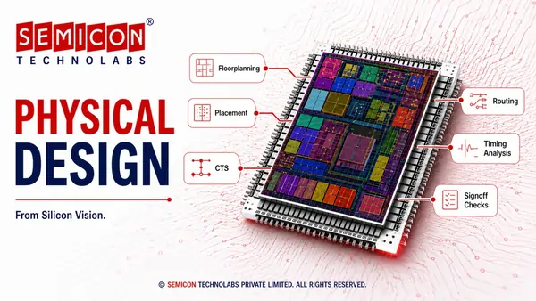
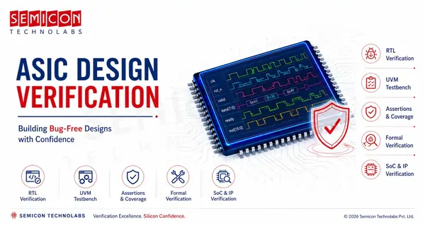
  • Kickstart your semiconductor career with Semicon Techno Labs. Learn Physical Design, Analog Layout, DFT, ASIC Verification, and Analog Circuit Design through industry-led training with placement support in Bangalore and Hyderabad.
    visit: https://semicontechs.com/analog-circuit-design/
    Kickstart your semiconductor career with Semicon Techno Labs. Learn Physical Design, Analog Layout, DFT, ASIC Verification, and Analog Circuit Design through industry-led training with placement support in Bangalore and Hyderabad. visit: https://semicontechs.com/analog-circuit-design/
    0 Comments 0 Shares 176 Views 0 Reviews
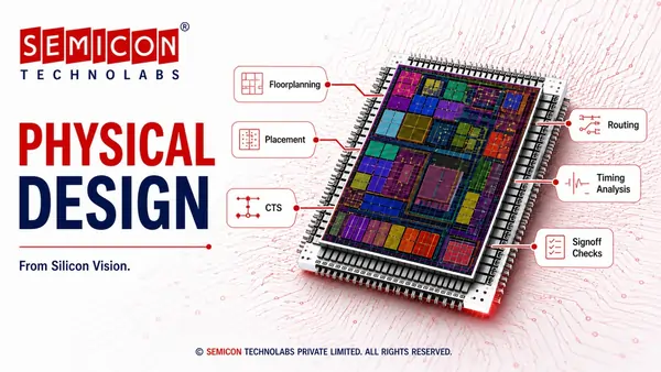
  • Kickstart your semiconductor career with Semicon Techno Labs. Learn Physical Design, Analog Layout, DFT, ASIC Verification, and Analog Circuit Design through industry-led training with placement support in Bangalore and Hyderabad.
    visit: https://semicontechs.com/
    Kickstart your semiconductor career with Semicon Techno Labs. Learn Physical Design, Analog Layout, DFT, ASIC Verification, and Analog Circuit Design through industry-led training with placement support in Bangalore and Hyderabad. visit: https://semicontechs.com/
    0 Comments 0 Shares 192 Views 0 Reviews
  • Automatic Bomb Calorimeter LZ-ABC-A100 - Fully Automatic Bomb Calorimeter

    Labozon Automatic Bomb Calorimeter measures calorific value over a 5–40 MJ/kg range using the isoperibol method with an 8-minute testing cycle.

    USB computer control, automatic water dosing, semiconductor refrigeration, and probe-based water measurement support laboratory testing.

    Designed for fuel, biomass, food, chemical, waste, and hydrocarbon analysis.

    #LabEquipment #AutomaticBombCalorimeter #BombCalorimeter
    #Calorimeter #Labozon

    https://www.labozon.com/automatic-bomb-calorimeter/lz-abc-a100
    Automatic Bomb Calorimeter LZ-ABC-A100 - Fully Automatic Bomb Calorimeter Labozon Automatic Bomb Calorimeter measures calorific value over a 5–40 MJ/kg range using the isoperibol method with an 8-minute testing cycle. USB computer control, automatic water dosing, semiconductor refrigeration, and probe-based water measurement support laboratory testing. Designed for fuel, biomass, food, chemical, waste, and hydrocarbon analysis. #LabEquipment #AutomaticBombCalorimeter #BombCalorimeter #Calorimeter #Labozon https://www.labozon.com/automatic-bomb-calorimeter/lz-abc-a100
    0 Comments 0 Shares 263 Views 0 Reviews
  • IC Curing Oven

    HJE Tech’s reliable IC Curing Oven offer precision temperature control & 24 heating zones. It has efficient curing for semiconductor & IC card manufacturing.
    https://www.hjetech.in/product/ic-curing-oven/
    IC Curing Oven HJE Tech’s reliable IC Curing Oven offer precision temperature control & 24 heating zones. It has efficient curing for semiconductor & IC card manufacturing. https://www.hjetech.in/product/ic-curing-oven/
    WWW.HJETECH.IN
    IC Curing Oven for Semiconductor and IC Card Manufacturing
    HJE Tech’s reliable IC Curing Oven offer precision temperature control & 24 heating zones. It has efficient curing for semiconductor & IC card manufacturing.
    0 Comments 0 Shares 93 Views 0 Reviews
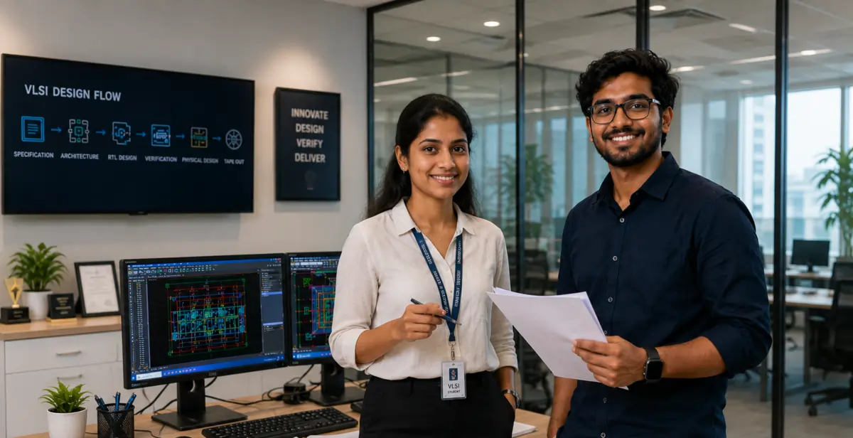
  • With over 30 years of combined industry experience, our instructors bring deep expertise in areas such as ASIC verification, physical design, DFT, analog layout, and VLSI design. Whether you are in Hyderabad or Bangalore, our VLSI training programs are hands-on, practical, and job-oriented, making us a preferred semiconductor training institute in both cities.
    visit: https://semicontechs.com/
    With over 30 years of combined industry experience, our instructors bring deep expertise in areas such as ASIC verification, physical design, DFT, analog layout, and VLSI design. Whether you are in Hyderabad or Bangalore, our VLSI training programs are hands-on, practical, and job-oriented, making us a preferred semiconductor training institute in both cities. visit: https://semicontechs.com/
    0 Comments 0 Shares 211 Views 0 Reviews
  • Lead Selenide Nanoparticles

    Searching for lead selenide nanoparticles with exceptional quality and consistent performance? NN Crystal US Corporation supplies premium lead selenide nanoparticles designed for advanced research, photonics, infrared detectors, and semiconductor applications. Our high-purity nanomaterials are manufactured to meet strict quality standards, helping researchers and industries achieve reliable, accurate, and innovative results across a wide range of scientific and technological projects.

    https://nn-labs.com/products/lead-selenide-quantum-dots-pbse
    Lead Selenide Nanoparticles Searching for lead selenide nanoparticles with exceptional quality and consistent performance? NN Crystal US Corporation supplies premium lead selenide nanoparticles designed for advanced research, photonics, infrared detectors, and semiconductor applications. Our high-purity nanomaterials are manufactured to meet strict quality standards, helping researchers and industries achieve reliable, accurate, and innovative results across a wide range of scientific and technological projects. https://nn-labs.com/products/lead-selenide-quantum-dots-pbse
    0 Comments 0 Shares 294 Views 0 Reviews
  • Master VLSI with Semicon Tech's expert-led training programs. Gain practical experience in ASIC Design, Physical Design, RTL Design, Verification, STA, DFT, and secure placement opportunities with leading semiconductor companies.
    visit: https://semicontechs.com/
    Master VLSI with Semicon Tech's expert-led training programs. Gain practical experience in ASIC Design, Physical Design, RTL Design, Verification, STA, DFT, and secure placement opportunities with leading semiconductor companies. visit: https://semicontechs.com/
    0 Comments 0 Shares 122 Views 0 Reviews
  • We are a leading provider of the best VLSI training, with expert-run centers in both Hyderabad and Bangalore. At Semicon Technolabs, we specialize in delivering high-quality, industry-focused VLSI training that equips students and professionals with the skills needed to succeed in the competitive semiconductor sector.
    visit: https://semicontechs.com/
    We are a leading provider of the best VLSI training, with expert-run centers in both Hyderabad and Bangalore. At Semicon Technolabs, we specialize in delivering high-quality, industry-focused VLSI training that equips students and professionals with the skills needed to succeed in the competitive semiconductor sector. visit: https://semicontechs.com/
    0 Comments 0 Shares 201 Views 0 Reviews
  • We are a leading provider of the best VLSI training, with expert-run centers in both Hyderabad and Bangalore. At Semicon Technolabs, we specialize in delivering high-quality, industry-focused VLSI training that equips students and professionals with the skills needed to succeed in the competitive semiconductor sector.
    visit: https://semicontechs.com/
    We are a leading provider of the best VLSI training, with expert-run centers in both Hyderabad and Bangalore. At Semicon Technolabs, we specialize in delivering high-quality, industry-focused VLSI training that equips students and professionals with the skills needed to succeed in the competitive semiconductor sector. visit: https://semicontechs.com/
    0 Comments 0 Shares 129 Views 0 Reviews
More Results